Highlights:
SAN JOSE, Calif., Oct. 6, 2015 — (PRNewswire) — Cadence Design Systems, Inc. (NASDAQ: CDNS) today announced the new Cadence® Tensilica® Vision P5 digital signal processor (DSP), its flagship high-performance vision/imaging DSP core. This imaging and vision DSP core offers up to 13X performance boost, with an average of 5X less energy usage on vision tasks compared to the previous generation IVP-EP imaging and video DSP.
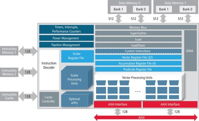
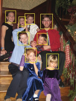
The Tensilica Vision P5 DSP is built from the ground up for applications requiring ultra-high memory and operation parallelism to support complex vision processing at high resolution and high frame rates. As such, it is ideal for off-loading vision and imaging functions from the main CPU to increase throughput and reduce power. End-user applications that can benefit from the DSP's capabilities include image and video enhancement, stereo and 3D imaging, depth map processing, robotic vision, face detection and authentication, augmented reality, object tracking, object avoidance and advanced noise reduction.
The Tensilica Vision P5 DSP core includes a significantly expanded and optimized Instruction Set Architecture (ISA) targeting mobile, automotive advanced driver assistance systems (or ADAS, which includes pedestrian detection, traffic sign recognition, lane tracking, adaptive cruise control, and accident avoidance) and Internet of Things (IoT) vision systems.
The advances in the Tensilica Vision P5 DSP further improve the ease of software development and porting, with comprehensive support for integer, fixed-point and floating-point data types and an advanced toolchain with a proven, auto-vectorizing C compiler. The software environment also features complete support of standard OpenCV and OpenVX libraries for fast, high-level migration of existing imaging/vision applications with over 800 library functions.
The Tensilica Vision P5 core includes these new features:
- Wide 1024-bit memory interface with SuperGather™ technology for maximum performance on the complex data patterns of vision processing
- Up to 4 vector ALU operations per cycle, each with up to 64-way data parallelism
- Up to 5 instructions issued per cycle from 128-bit wide instruction delivering increased operation parallelism
- Enhanced 8-,16- and 32-bit ISA tuned for vision/imaging applications
- Optional 16-way IEEE single-precision vector floating-point processing unit delivering a massive 32GFLOPs at 1GHz
For more information on the Tensilica Vision P5 DSP, visit http://www.cadence.com/news/TensilicaVisionP5.
"There is an explosion in vision processing applications that require dedicated, efficient offload processors to handle the large streams of data in real time," stated Jeff Bier, co-founder and president of Berkeley Design Technology, Inc. (BDTI). "Processor innovations like the Tensilica Vision P5 DSP help provide the backbone required for increasingly complex vision applications."
"The need for a more efficient but powerful processor is necessary for mobile devices transitioning into 4K resolution," stated Jon Peddie, founder of Jon Peddie Research. "This recent announcement of a new vision processor is essential for enabling next-generation devices."
"Imaging algorithms are quickly evolving and becoming much more complex – particularly in object detection, tracking and identification," stated Chris Rowen, CTO of the IP Group at Cadence. "Additionally, we are seeing a lot more integrated systems with multiple sensor types, feeding even more data in for processing in real time. These highly complex systems are driving us to provide more performance in our DSPs than ever before, at even lower power. The Tensilica Vision P5 DSP is a major step forward to meeting tomorrow's market demands."
The Tensilica Vision P5 DSP is based on the Cadence Tensilica Xtensa® architecture, and combines flexible hardware choices with a library of DSP functions and numerous vision/imaging applications from our established ecosystem partners. It also shares the comprehensive Tensilica partner ecosystem for other applications software, emulation and probes, silicon and services and much more. The Xtensa architecture is the second most popular licensable processor architecture, shipping at a rate of over 2B cores per year in products spanning sensors to supercomputers.
About Cadence
Cadence enables global electronic design innovation and plays an essential role in the creation of today's integrated circuits and electronics. Customers use Cadence software, hardware, IP and services to design and verify advanced semiconductors, consumer electronics, networking and telecommunications equipment, and computer systems. The company is headquartered in San Jose, Calif., with sales offices, design centers and research facilities around the world to serve the global electronics industry. More information about the company, its products and its services is available at
http://www.cadence.com.
© 2015 Cadence Design Systems, Inc. All rights reserved worldwide. Cadence, the Cadence logo, Tensilica, and Xtensa are registered trademarks and SuperGather is a trademark of Cadence Design Systems, Inc. in the United States and other countries. All other trademarks or registered trademarks are those of their respective holders.
This news release contains certain forward-looking statements, including expectations about industry and market developments and trends, that are based on our current expectations and involve numerous risks and uncertainties that may cause these forward-looking statements to be inaccurate. Risks that may cause these forward-looking statements to be inaccurate include among others: market trends may change, current expectations about future technology needs or industry developments may prove inaccurate, or the other risks detailed from time-to-time in our Securities and Exchange Commission filings and reports, including, but not limited to, our most recent quarterly report on Form 10-Q and our annual report on Form 10-K. We do not intend to update the information contained in this press release.
QUOTE SHEET
"We have a long-standing relationship with Cadence and have successfully used other Tensilica technologies such as the Xtensa processor for our high-performance and ultra-low power IoT sensor hub IC," said Kenji Nakamura, corporate officer/deputy general manager of MegaChips. "As a market leader in application-specific standard product (ASSP) solutions, we see vision and imaging as the next growth applications areas requiring high-performance, low-power DSPs. We are excited to be a Cadence partner as they make huge investments in imaging and vision DSP advancements, which are built on the proven Xtensa processors and its development tools."
"Being a leader in imaging and vision software for mobile platform, Morpho continuously invests in partnering with companies that provide advanced technologies," said Masayuki Urushiyama, executive vice president of Global Sales & Marketing of Morpho. "The new Tensilica Vision P5 DSP significantly improved the power and performance of our imaging software, enabling us to optimize our solution for end-user applications that utilize functionalities such as video stabilization and wide dynamic range."
"By porting our fog removal software to the new Tensilica Vision P5 DSP, we achieved 85X performance improvement, with 25X less power consumption," said Shanti Swarup, chief technology officer at Uurmi Systems. "We utilized Cadence's extensive software library and ISS simulator to quickly port our technology. The total turnaround time was less than five weeks and we achieved dramatic improvement in power and performance, which enabled us to sell our software to the embedded systems market."
For more information, please contact:
Cadence Newsroom
408-944-7039
Email Contact


Photo -
http://photos.prnewswire.com/prnh/20151002/273545
Photo -
http://photos.prnewswire.com/prnh/20151002/274228
Logo -
http://photos.prnewswire.com/prnh/20140102/SF39436LOGO
To view the original version on PR Newswire, visit: http://www.prnewswire.com/news-releases/new-cadence-tensilica-vision-p5-dsp-enables-4k-mobile-imaging-with-13x-performance-boost-and-5x-lower-energy-300154540.html
SOURCE Cadence Design Systems, Inc.
| Contact: |
| Cadence Design Systems, Inc.
Web: http://www.cadence.com |


