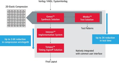
Physically aware 2D Elastic Compression architecture reduces test logic wirelength by up to 2.6X and enables compression ratios to scale beyond 400X without impacting design size
SAN JOSE, Calif., Feb. 2, 2016 — (PRNewswire) — Cadence Design Systems, Inc. (NASDAQ: CDNS) today announced the new Modus™ Test Solution that enables design engineers to achieve an up to 3X reduction in test time, thereby reducing production test cost and increasing silicon profit margins. This next-generation test solution incorporates patent-pending, physically aware 2D Elastic Compression architecture that enables compression ratios beyond 400X without impacting design size or routing.
To address the challenges that come with testing designs, the Cadence® Modus Test Solution includes the following innovative capabilities:
- 2D compression: Scan compression logic forms a physically aware two-dimensional grid across the chip floorplan, enabling higher compression ratios with reduced wirelength. At 100X compression ratios, wirelength for 2D compression can be up to 2.6X smaller than current industry scan compression architectures.
- Elastic compression: Registers embedded in the decompression logic enable fault coverage to be maintained at compression ratios beyond 400X by controlling care bits sequentially across multiple scan cycles during automatic test pattern generation (ATPG).
- Embedded memory bus support: A shared test access bus can be inserted to perform at-speed programmable memory built-in self test (PMBIST) across multiple embedded memories in an IP core. New soft programmable test algorithms for FinFET SRAMs and automotive safety applications are also included with this feature.
- Powerful common scripting and debug environment: Design for test (DFT) logic insertion and ATPG capabilities use a new, unified Tcl scripting and debug environment that is shared with the Cadence Genus™ Synthesis Solution, the Innovus™ Implementation System and the Tempus™ Timing Signoff Solution.
"Our next-generation Modus Test Solution delivers new, innovative patent-pending technology that fundamentally changes the way design and test engineers address the test problem," said Dr. Anirudh Devgan, senior vice president and general manager of the Digital and Signoff Group at Cadence. "By using a physically aware approach in a 2D grid, and compressing patterns sequentially as well, the Modus Test Solution can significantly reduce digital test time in comparison to traditional approaches, thereby giving Cadence customers yet another significant profitability advantage."
For more information on the Modus Test Solution, please visit www.cadence.com/news/modus.
Customer Endorsements
"The Modus Test Solution demonstrated a 3.6X reduction in test time on a customer networking chip without impacting design routability or fault coverage. This technology definitely reduces production test costs. The evolution of the Modus Test Solution, as well as the Innovus Implementation System, the Tempus Timing Signoff Solution and the Voltus™ IC Power Integrity Solution, provides a leading-edge end-to-end design flow in 14nm and beyond for our worldwide design centers and for our ASIC customers. "
-Sue Bentlage, director, ASIC design and methodology at GLOBALFOUNDRIES
"Minimizing the cost of test is crucial in high-volume, price-sensitive markets like embedded processing. The Modus Test Solution is showing a 1.7X reduction in digital test time on one of our largest and most complex embedded processor chips without any impact on design closure."
-Roger Peters, MCU silicon development at Texas Instruments
"With the Modus Test Solution, we achieved an impressive 2.6X reduction in compression wirelength and a 2X reduction in scan time. The reduction in compression logic wirelength enabled us to address a key challenge for design closure as we push to smaller process nodes and scale design size."
-Alan Nakamoto, vice president, engineering services at Microsemi Corp.
"Test time has a significant impact on semiconductor product costs and production capacity, so reducing test time is important. We have seen the Modus Test Solution achieve a 2X reduction in test time without impacting fault coverage or die size."
-Chris Malkin, baseband IC manager at Sequans
About Cadence
Cadence enables global electronic design innovation and plays an essential role in the creation of today's integrated circuits and electronics. Customers use Cadence software, hardware, IP and services to design and verify advanced semiconductors, consumer electronics, networking and telecommunications equipment, and computer systems. The company is headquartered in San Jose, Calif., with sales offices, design centers and research facilities around the world to serve the global electronics industry. More information about the company, its products and its services is available at www.cadence.com.
© 2016 Cadence Design Systems, Inc. All rights reserved worldwide. Cadence and the Cadence logo are registered trademarks and Genus, Innovus, Modus, Tempus, and Voltus are trademarks of Cadence Design Systems, Inc. in the United States and other countries. All other trademarks are the property of their respective owners.
For more information, please contact:
Cadence Newsroom
408-944-7039
Email Contact

Photo -
http://photos.prnewswire.com/prnh/20160201/328500
Logo -
http://photos.prnewswire.com/prnh/20140102/SF39436LOGO
To view the original version on PR Newswire, visit: http://www.prnewswire.com/news-releases/new-cadence-modus-test-solution-delivers-up-to-3x-reduction-in-soc-test-time-300213455.html
SOURCE Cadence Design Systems, Inc.
| Contact: |
| Cadence Design Systems, Inc.
Web: http://www.cadence.com |