Successful silicon bring-up extends leadership in chiplet-enabled silicon solutions to accelerate AI connectivity and compute
LONDON & TORONTO — (BUSINESS WIRE) — March 11, 2024 — Alphawave Semi (LSE: AWE), a global leader in high-speed connectivity and compute solutions for the world’s technology infrastructure, today announced the successful bring-up of its first chiplet-connectivity silicon platform on TSMC’s most advanced 3nm process. This new silicon-proven Universal Chiplet Interconnect Express (UCIeTM) subsystem expands Alphawave Semi’s portfolio and leadership in connectivity silicon. It paves the way for a robust, open chiplet ecosystem that accelerates connectivity and compute for high-performance AI systems. An industry-first live demo of Alphawave Semi’s 24Gbps UCIe silicon platform on the TSMC 3nm process was recently unveiled at the Chiplet Summit in Santa Clara, CA.
This press release features multimedia. View the full release here: https://www.businesswire.com/news/home/20240311461384/en/

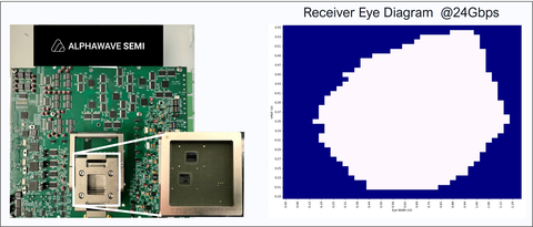
Alphawave Semi 24Gbps UCIe 3nm silicon platform (Graphic: Business Wire)
Alphawave Semi’s 3nm UCIe complete PHY + Controller subsystem is capable of 24Gbps data rates, delivering high bandwidth density at extremely low power and low latency. The solution is compliant with the latest UCIe Revision 1.1 Specification and includes a highly configurable Die-to-Die D2D controller that supports streaming, PCIe®/CXLTM, AXI-4, AXI-S, CXS, and CHI protocols. The subsystem features Bit Error Rate (BER) Health Monitoring to ensure reliable operation. The PHY can be configured to support TSMC’s advanced packaging technologies such as Chip-on-Wafer-on-Substrate (CoWoS®) and Integrated Fan-Out (InFO) which maximize signal densities, as well as organic substrates for a more cost-effective solution.
“We’re pleased with the results of our latest collaboration with Alphawave Semi in the delivery of a silicon-proven chiplet-connectivity solution on TSMC’s 3nm process,” said Dan Kochpatcharin, head of the Design Infrastructure Management Division at TSMC. “We will continue to work with our Open Innovation Platform® (OIP) partners like Alphawave Semi to help foster a robust and open chiplet ecosystem for high-performance connectivity and compute silicon solutions to enable more AI applications.”
“Achieving 3nm silicon-proven status for our 24Gbps UCIe subsystem is a key milestone for Alphawave Semi, as it is an essential piece of our chiplet connectivity platform tailored for hyperscaler and data-infrastructure applications,” said Letizia Giuliana, VP IP Product Marketing at Alphawave Semi. “We are thankful to our TSMC team for their outstanding support, and we look forward to accelerating our mutual customers' high-performance chiplet-based designs on TSMC's leading-edge 3nm process.”
For more information, visit http://awavesemi.com.
Customers can benefit from Alphawave Semi’s application-optimized IP subsystems and advanced 2.5D/3D packaging expertise through the integration of advanced interfaces such as UCIe, PCIe, CXL, Multi-Standard-Serdes, and HBM onto custom chips and chiplets.
About Alphawave Semi
Alphawave Semi is a global leader in high-speed connectivity and compute silicon for the world's technology infrastructure. Faced with the exponential growth of data, Alphawave Semi's technology services a critical need: enabling data to travel faster, more reliably, and with higher performance at lower power. We are a vertically integrated semiconductor company, and our IP, custom silicon, and connectivity products are deployed by global tier-one customers in data centers, compute, networking, AI, 5G, autonomous vehicles, and storage. Founded in 2017 by an expert technical team with a proven track record in licensing semiconductor IP, our mission is to accelerate the critical data infrastructure at the heart of our digital world. To find out more about Alphawave Semi, visit: awavesemi.com.
Alphawave Semi and the Alphawave Semi logo are trademarks of Alphawave IP Group plc. All rights reserved.
View source version on businesswire.com: https://www.businesswire.com/news/home/20240311461384/en/
Contact:
Gravitate PR for Alphawave Semi
alphawave@gravitatepr.com


