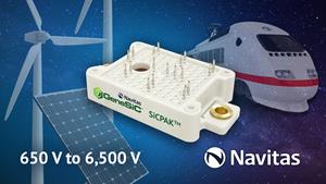
TORRANCE, Calif., May 08, 2023 (GLOBE NEWSWIRE) -- Navitas Semiconductor (Nasdaq: NVTS), the only pure-play, next-generation power semiconductor company, announces their expanded portfolio into higher power markets with their leading-edge silicon carbide (SiC) power products in SiCPAK™ modules and bare die.
Target applications cover centralized and string solar inverters, energy storage systems (ESS), industrial motion, electric vehicle (EV) on-board chargers, EV roadside fast chargers, wind energy, UPS, bi-directional microgrids, DC-DC converters, and solid-state circuit breakers.
Ranging from 650 V to 6,500 V, Navitas has the widest range of SiC technology. From an original line-up of discrete packages - from 8x8 mm surface-mount QFNs to through-hole TO-247s - the GeneSiC SiCPAK is an initial, direct entry point into higher-power applications. A comprehensive power-module roadmap, with high-voltage SiC MOSFETs and MPS diodes, GaN power ICs, high-speed digital isolators and low-voltage silicon control ICs is being mapped out.
Dr. Ranbir Singh, Navitas EVP for SiC noted, “With a complete portfolio of leading-edge power, control and isolation technology, Navitas will enable customers to accelerate the transition from fossil fuels, and legacy silicon power products to new, renewable energy sources and next-generation semiconductors, with more powerful, more efficient, faster-charging systems.”
SiCPAK™ modules employ ‘press-fit’ technology to offer compact form factors for power circuits and deliver cost-effective, power-dense solutions to end users. The modules are built upon GeneSiC die that have already made a mark in terms of superior performance, reliability, and ruggedness. Examples include a SiCPAK half-bridge module, rated at 6 mOhm, 1,200 V with industry-leading trench-assisted planar-gate SiC MOSFET technology. Multiple configurations of SiC MOSFETs and MPS diodes will be available to create application-specific modules for superior system performance. The initial release will include 1,200 V-rated half-bridge modules in 6, 12, 20, and 30mOhm ratings.
Within the lead-free SiCPAK, each SiC chip is silver (Ag) sintered to the module’s substrate for superior cooling and reliability. The substrate itself is ‘direct-bonded copper’ (DBC) and manufactured using an active-metal brazing (AMB) technique on silicon-nitride (Si3N4) ceramics, ideal for power-cycling applications. This construction delivers excellent strength and flexibility, fracture resistance, and good thermal conductivity for cool, reliable, long-life operation.
For customers who prefer to make their own high-power modules, all GeneSiC MOSFET and MPS diodes are available in bare die format, with gold (Au) and aluminum (Al) top-side metalizations.
Parts are available now to qualified customers. Please contact sicsales@navitassemi.com for more information.
About Navitas
Navitas Semiconductor (Nasdaq: NVTS) is the only pure-play, next-generation power-semiconductor company, founded in 2014.
GaNFast™ power ICs integrate gallium nitride (GaN) power and drive, with control, sensing, and protection to enable faster charging, higher power density, and greater energy savings. Complementary
GeneSiC™ power devices are optimized high-power, high-voltage, and high-reliability silicon carbide (SiC) solutions. Focus markets include mobile, consumer, data center, EV, solar, wind, smart grid, and industrial. Over 185 Navitas patents are issued or pending. Over 75 million GaN and 10 million SiC units have been shipped, and Navitas introduced the industry’s first and only 20-year GaN warranty. Navitas was the world’s first semiconductor company to be
CarbonNeutral®-certified.
Navitas, GaNFast, GaNSense, GeneSiC, SiCPAK, and the Navitas logo are trademarks or registered trademarks of Navitas Semiconductor and subsidiaries. All other brands, product names, and marks are or may be trademarks or registered trademarks used to identify products or services of their respective owners.
Contact Information:
Stephen Oliver, VP Corporate Marketing & Investor Relations, ir@navitassemi.com
A photo accompanying this announcement is available at https://www.globenewswire.com/NewsRoom/AttachmentNg/f0aefc1b-6d55-41e1-84bb-f0207f441451


