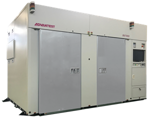
TOKYO, Oct. 10, 2018 (GLOBE NEWSWIRE) -- Leading semiconductor test equipment supplier Advantest Corporation (TSE: 6857) has announced its next-generation B6700D memory burn-in tester to meet growing global customer demand for server and mobile data-storage solutions during the memory market’s current super cycle. By measuring the functions of NAND flash and DRAM memory devices during burn-in, this new tester delivers both high throughput and a low cost of test.
With the semiconductor memory market expected to grow significantly in the future, chip makers require a fast, high-volume test solution to keep pace with their customers’ growing demand. The dual-chamber B6700D fulfills this need by testing as many as 48 burn-in boards in parallel at speeds up to 10 MHz, which helps memory producers get their newest products to market faster while also reducing testing costs.
This new memory burn-in tester uses a high-capacity power supply that delivers a maximum of 256 amps per burn-in board – twice that of the first-generation B6700 tester. In addition, the B6700D has twice the driver pin resources as its predecessor, enabling it to reach higher testing frequencies.
In another advance over its predecessor, the B6700D can maintain or increase parallelism to keep throughput high as the number of stacked NAND die per package increases in the future. Additionally, the B6700D’s oven can replicate operating conditions while controlling temperature to within one tenth of a degree.
The new B6700D runs on the same operating system as the earlier B6700, making the testers fully compatible. The bad block memory (BBM), universal buffer memory (UBM) and data pattern memory (DPM) functions are supported to enable NAND device testing.
Shipments to customers have begun and additional orders are being accepted.
About Advantest Corporation
A world-class technology company, Advantest is the leading producer of automatic test equipment (ATE) for the semiconductor industry and a premier manufacturer of measuring instruments used in the design and production of electronic instruments and systems. Its leading-edge systems and products are integrated into the most advanced semiconductor production lines in the world. The company also focuses on R&D for emerging markets that benefit from advancements in nanotech and terahertz technologies, and has introduced multi-vision metrology scanning electron microscopes essential to photomask manufacturing, as well as a groundbreaking 3D imaging and analysis tools. Founded in Tokyo in 1954, Advantest established its first subsidiary in 1982, in the USA, and now has subsidiaries worldwide. More information is available at
www.advantest.com.
ADVANTEST CORPORATION
3061 Zanker Road
San Jose, CA 95134, USA
Judy Davies
Judy.davies@advantest.com
A photo accompanying this announcement is available at http://www.globenewswire.com/NewsRoom/AttachmentNg/da7e5b0a-aa87-4749-a84d-81a210288b35


